Mar 13,2024
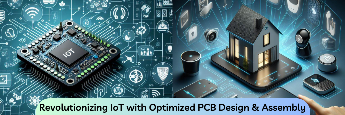
Since its inception, the Internet of Things, or IoT, has revolutionized many industries, and the electronics industry is no exception. Technology is ushering in an era where devices we use in our daily lives are smart and interconnected. Complex printed circuit boards (PCBs) are a crucial and integral part of IoT devices, allowing them to function as intended. They transform hardware components into smart, interconnected devices capable of sensing, processing, and transforming data. Also, they enable compact, energy-efficient designs required for IoT devices where size and power consumption are paramount. Considering their immense significance in IoT applications, paying extra attention to PCB design and assembly is important. Would you like to know how to optimize PCB design and assembly for IoT devices? This post highlights essential PCB design and assembly guidelines tailored to meet unique requirements of IoT applications.

Essential PCB Design and Assembly Guidelines for IoT Applications
The following pointers should be considered when designing and assembling circuit boards for IoT devices. These pointers may help in minimizing errors during the process.
-
Determine Application Requirements: The first and most crucial step is understanding the specific requirements of IoT applications. Different applications have different specifications depending on the areas where they are used. Before making any firm decision, consider form factor, communication protocol, power consumption, environmental conditions, and other related factors.
-
Component Selection and Placement: Component selection and placement are another essential consideration. Choose components with compact, power-efficient, and long lifespan to ensure the longevity of IoT device. Once done with the selection part, it is equally important to pay attention to its proper placement. Minimize trace lengths and reduce signal interference by placing critical components close to the microcontroller or processor. Avoid placing sensitive analog components near noisy digital ones.
-
Wireless Connectivity: Most of the times, IoT devices depend on wireless communication. Thus, carefully consider wireless modules when designing PCBs for IoT applications. Make sure that the PCB layout covers antenna placement, interference mitigation, signal integrity, and so on. Implementing thorough testing procedures is essential to verify ’reliability and range of wireless connectivity.
-
Signal Integrity: IoT devices often involve sensitive sensors and communication interfaces. Thus, signal integrity is critical for IoT devices. Signal integrity can be maintained using appropriate impedance matching techniques, minimizing signal trace length, using power planes to provide a stable reference for signal traces, and more.
-
Power Management: This is a cornerstone of IoT design. This can be achieved using low-power components and utilizing sleep modes when the device is idle. Consider using power switching circuits and voltage regulators for efficient power management. Also, implement energy harvesting techniques such as solar panels or piezoelectric elements for IoT devices in remote locations.
-
Design for Manufacturing (DFM): It is vital to follow DFM guidelines to ensure a cost-effective and efficient PCB assembly. These guidelines include using standard PCB sizes and materials to reduce overall production costs, ensuring that components footprints and assembly tolerance meet manufacturing capabilities, minimizing unique components to simplify sourcing, and more.
-
Environmental Considerations: Depending on the application requirement, IoT devices are used in different settings – indoor and outdoor. PCB should be designed keeping environmental factors in mind, such as humidity, temperature, exposure to dust or moisture, and more. Also, consider conformal coating or ruggedized enclosures to protect them from adverse conditions.
-
Test and Quality Assurance: Once done with the designing part, it is important to perform thorough testing. This will help identify errors or bugs early and ensure your IoT devices perform reliably. Functional testing, thorough inspection of solder joints, and in-circuit testing (ICT) are widely used testing techniques.
-
Compliance and Certification: IoT devices must meet regulatory and certification standards such as FCC, CE, or UL. The PCB design must comply with these standards. Achieving electromagnetic compatibility is a crucial aspect and EMI mitigation techniques such as filtering, shielding, and grounding may be used to ensure safety and EMC-enabled IOT devices.
PCB designing and assembly is a complex process, and needs to be executed properly to avoid possible errors. The abovementioned guidelines may help create reliable, efficient, cost-effective boards and assemblies for IoT devices. In case of any technical assistance, one must consult an industry-leading
PCB manufacturer and assembly service provider in chicago. Creative Hi-tech stands tall among its other competitors. With years of industry experience, the company offers high-quality PCB design and assembly services for IoT and other applications. The experts at the company can also assist you in selecting the appropriate PCB materials after analyzing the specifications and requirements.


